
The journey of a semiconductor integrated chip (IC) begins with the design of the IC, manufacturing of the wafer by imprinting the circuits and devices into the semiconductor wafer, separation of the chips into the individual units and finally assembling & packaging of the chips and other electronic active & passive components to function them as an electronic device. Each individual processes involved are ultra-complex in nature and thus detail understanding of it is of utmost importance.
During assembly and packaging of the semiconductor devices, one overlooked part in assembly is Die Preparation (Die Prep) process. While functionality and end quality of the products are the end goals for the semiconductor companies, getting it from fab to final assembly line is often an under appreciated step in the IC supply chain. The Die Prep process essentially involves multiple steps and encompasses wafer thinning (backgrinding), wafer singulation and pick & place in a nut-shell. Each process also accompanies with its own metrology process to ensure quality and yield. Due to the complex nature of the wafers & devices, each sub-process are equally crucial and involves highly sophisticated materials & equipments for successful processing. Optimum Die Prep process not only ensures quality of the dies but also helps to lower the cost and also prevents unexpected assembly hiccups.

Wafer Backgrinding/ Wafer Thinning
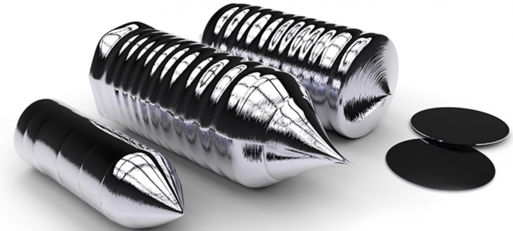
Wafer backgrinding is a process of removing material from the backside of a wafer to a desired final target thickness while active devices are already fabricated on the wafer front side. This produces a thinner wafer which ultimately helps to manufacture a thinner package. In the advanced packaging technology, wafer thinning is applied in various process steps for the fabrication of the semiconductor devices and helps to achieve further miniaturization & increased performance.
Wafers get fabricated in standard thickness range and then devices are made in front-end wafer process . The wafers then thinned down during back-end of the wafer process or in assembly process. The original wafer thickness is a function of wafer diameter and provides a strength to the wafer during manufacturing handling.
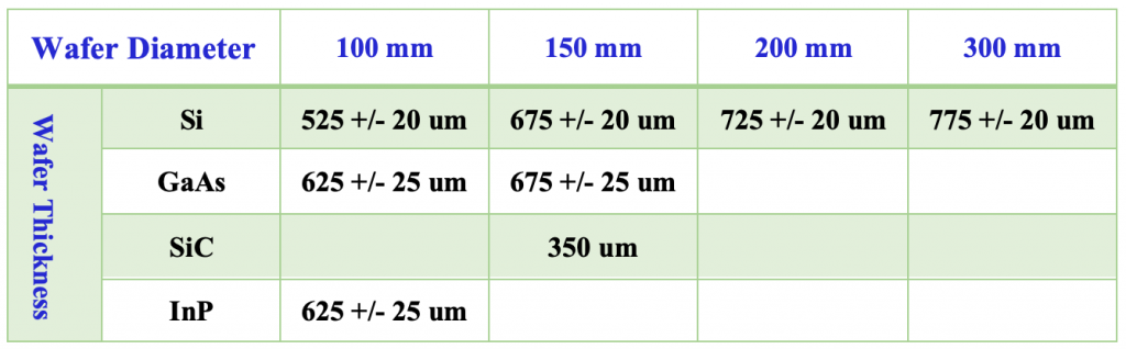
Wafer thinning is implemented during different process steps as the wafer moves into the manufacturing process flow. After the ingot first gets sliced into the individual wafer, the wafer will be planarized multiple times during the front-end of line (FEOL) manufacturing process. However, the main wafer thinning happens during the back-end of line (BEOL) process at the packaging level and is generally referred as wafer backgrinding.
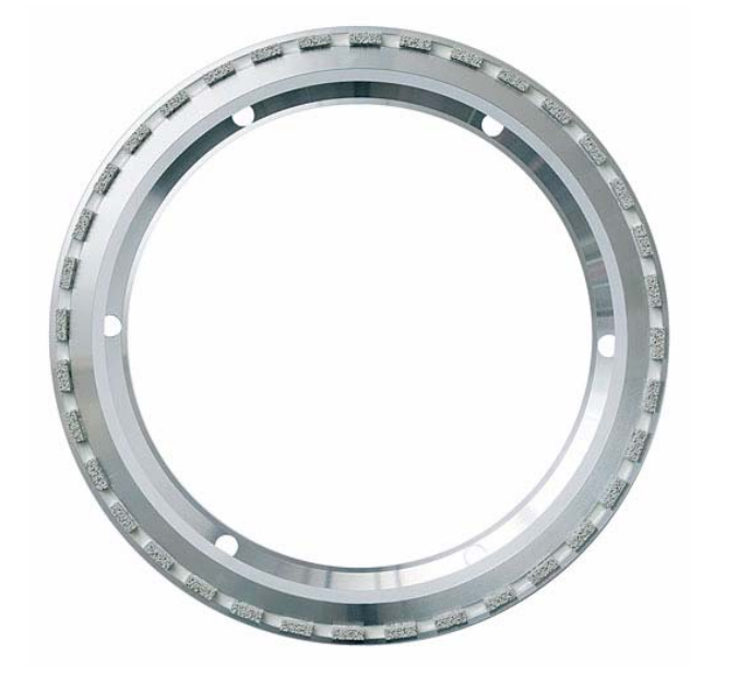
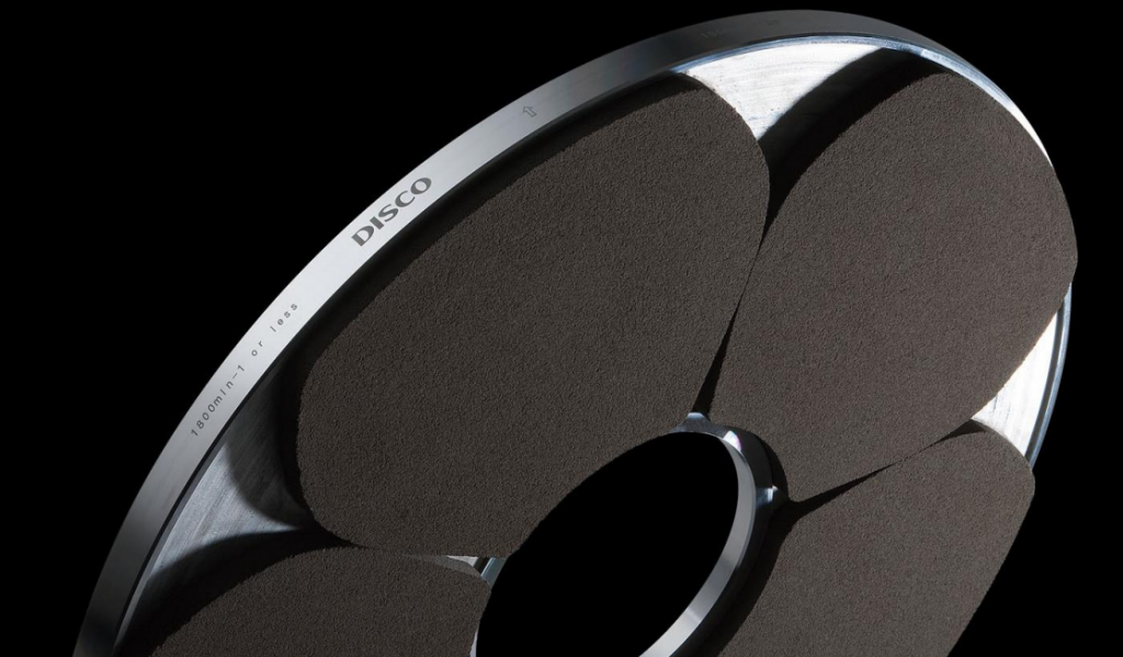
At present, there are various wafer thinning technology available on the market and the choice of the technique is dependent upon the type of the substrate material, wafer final thickness and the cost. In terms of equipment; grinding & polishing are the two main equipment categories used in the wafer thinning. For grinding, grinding wheels are used and are made of diamond based fixed abrasives bonded with either resin, vitrified or metal bond. For polishing, pad/wheel with fixed or free abrasives as well as slurry will be used. New generation of the equipment such as Disco DGP8761 combines both grinding and polishing (wet or dry) step to produce wafer as thin as 20um. At present DISCO (Japanese company) is a market leader for both the grinding and CMP equipment. Besides DISCO, REVASUM (US based – supplies both grinding & CMP equipment), EBARA (Japanese company – CMP equipment), APPLIED MATERIALS (US based – CMP equipment) and ACCRETECH (Japanese company – supplies both grinding & CMP equipment) are the suppliers of the grinding & CMP equipment.
Thinning process mostly involves standard grinding and polishing. Polishing can be chemical- mechanical planarization (CMP), dry polishing or wet etching. The final polishing provides a stress relief and removes any micro-crack or subsurface damage created during the grinding process.
The most common methods of thinning are backgrinding with conventional grinding wheels, followed by fine polishing such as CMP, dry polishing and wet etching to reduce surface defects and relieve grinding induced stress. During grinding, grinders rotates the wafer placed on a vacuum chuck and feed the rotating grinding wheel into the backside of the wafer. The wafer passes rough and fine grinding steps that reduces the thickness of the wafer as required.
TAIKO process
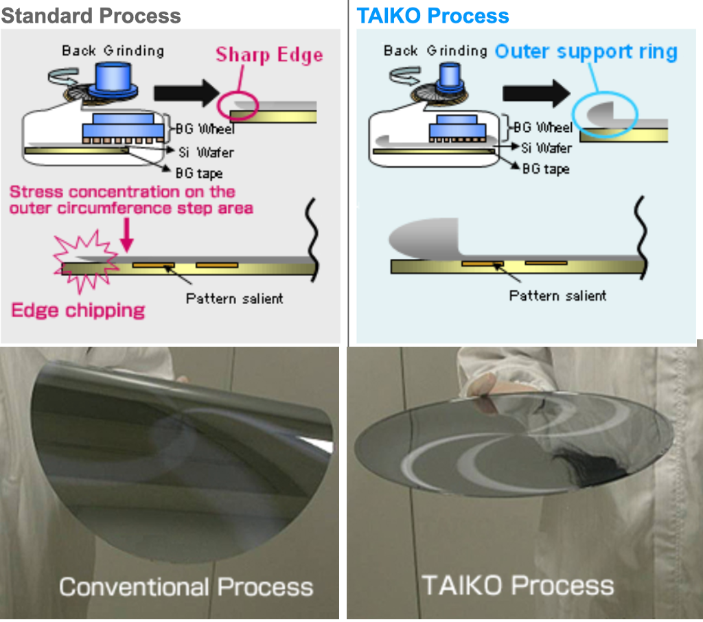
Taiko process is a wafer backgrinding method developed by DISCO as a solution to solve the wafer handling and edge chipping challenges in conventional grinding process. This grinding method leaves an approximately 3mm wide frame on the outer circumference of the wafer and thin grinds only the inner circumference of the backside of the wafer. The remaining thick edge ring reduces the risk of wafer breakage during handling by lowering the wafer warpage and providing crack free edge.
A protective film is typically applied on the device side of the wafer to secure the die during thinning.
• Die strength and smoothness can be increased based on grit/slurry selection of the grinding wheels, while also decreasing warpage and subsurface damage.
• Lower cost, higher throughput are the key advantage whereas higher surface roughness and handling of ultrathin wafers are the key challenges of mechanical grinding.
• Probed wafers comes out of the wafer sort. The wafers will go through the wafer frontside BG tape mount, wafer backgrind, dicing tape mount & BG tape removal process. BG Tape selection is based on the bump height as BG tape needs to encapsulate the bump completely.
- Grinding wheels : In general, grinding typically involves Z1 & Z2 grinding wheels where Z1 is coarse grinding ( < #500 grit grinding wheel) and removes most of the Silicon (~ 500 – 600um). Z2 grinding is a fine grinding process ( typically < #3000 grit grinding wheel, but can be little finer) and removes about 20-50um of Silicon. If mirror finish is needed, Z3 wheel with much finer grit will be used.
- BG Tape Mount: Optimum laminate speed & roller pressure are the critical process parameters for the good tape mount.
- Wafers <100um thin will require Z3 fine grind processing in order to release grinding stress and achieve good die break strength.
- Monitor wafers will be run to check the process and tool health if : machine is idle for 24 hrs. or more, every machine maintenance or any engineering works.
- Quality Check (QC) at Backgrind – Typically, 1st wafer for every lot – manual 1x visual inspection.
Key failure mechanism – Conventional wafer backgrinding process can cause different type of failure in the wafer such as micro-crack, wafer warpage, wafer edge chipping and residual & mechanical stress resulting in wafer/die cracking & chipping.
Wafer Singulation
Wafer singulaiton is one of the key assemebly process & is getting more & more challenging with the next generation of the devices . Form factor reduction, incorporation of the low-k dielectric material in the wafer BEOL process and increasing metal density in the wafer street area makes the singulation process extremely challenging. In general, mechanical blade dicing, laser+saw hybrid dicing, stealth dicing, plasma dicing, laser full cut dicing etc. are established methods of dicing in the industry. Depending upon the wafer structure, cost, throughput and end quality requirement; one can choose appropriate wafer singulaiton method that meets quality and yield requirement.
• Singulation is the process of isolating individual dies from a wafer.
• The most common methods of wafer singulation are mechanical blade dicing, laser dicing, hybrid dicing involving laser and saw, scribe and break, and dice before grind (DBG) whereas stealth dicing, plasma dicing, laser full cut etc. are key advanced dicing options.
• Mechanical blade dicing is the traditional method of singulating die utilizing a diamond embedded blade to remove material while process water cools the blade and workpiece .
• While more robust, cheaper and flexible than other methods, mechanical dicing does produce a large kerf and chipping & are inherent part of the process.
• In mechanical blade dicing, street width governs the blade/kerf width.
• Total thickness (including bumps) of the wafer determines blade exposure in which blade exposure is restricted by blade width.
• The narrower the blade, smaller the exposure. Therefore, for wafers with narrower streets, thinning is required.
• For mechanical dicing, the process water is also critical to maintaining overall die quality. Moreover, process water temperature must be maintained at or below room temperature, preferably chilled, to help ensure planarity of the dicing chuck table & cool down the dicing blade.
• Surfactant injected into water assists cleanliness by suspending dicing particles on the wafer surface, making the debris easier to wash off. Additionally, some surfactants provide the added benefit of containing corrosion inhibitors.
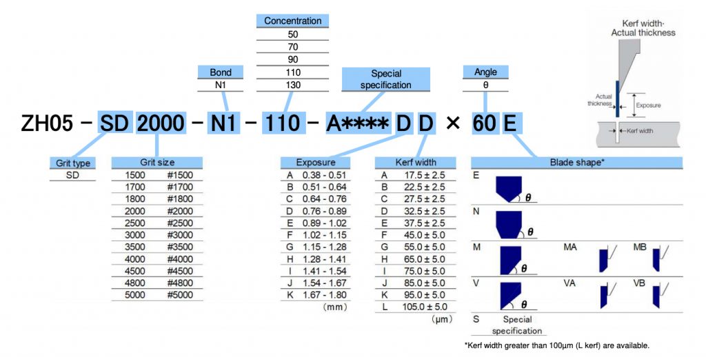
• Right blade selection with the proper ( diamond mesh size/concentration, bond material, kerf width) is the key to the successful dicing.
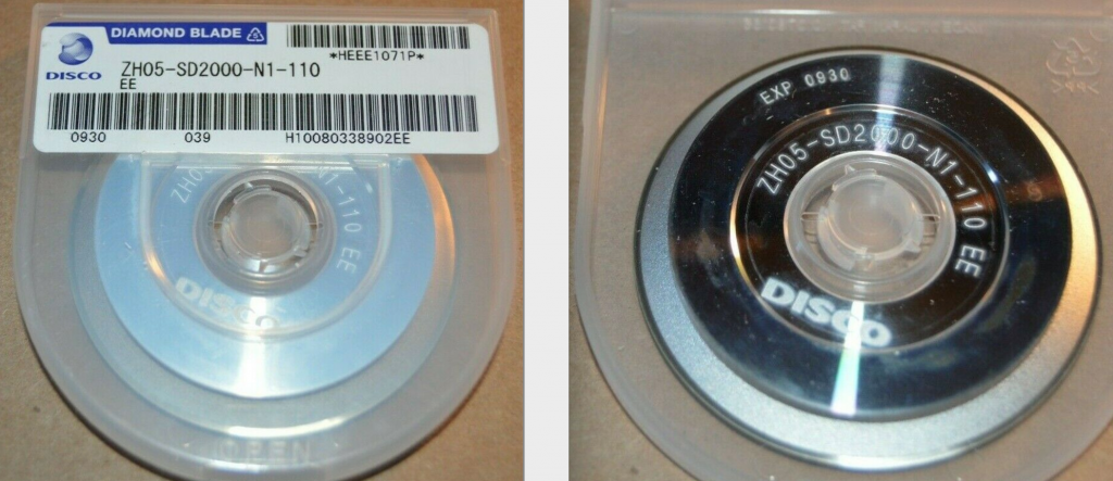
Dicing blade from Disco : ZH05-SD2000-N1-110-DD
Die Pick & Place
Process flow: Singulated die on wafer film (mylar) frame –> Mylar expansion –> Wafer/die alignment –> Pick collet/bond head alignment –> Die ejector –> Pick collet suction –>Die ejection –> pick & placement on the reel.
• Dies will be picked based on the input AOI map with multiple binning into tape and reel, gel paks & waffle packs.
• Loaded wafer will get expanded on the loading table. The operator/tool will perform the following actions- local angle correction, multiple point pitch measurements, frame angle check, learn first die and direction to pick die as part of the recipe teach and proceeds to pick the dies.
• Full inspection for die back and front active area with different cameras vision system during pick and placement process. Vision system will have side wall inspection with optional IR inspection capability.
• Components are placed in the carrier tape cavities and held in place by the cover tape, which is sealed on both sides of the carrier.
• Cover tape should not extend past the edge of the carrier tape. Tapes in adjacent layers should not stick together when wound on the carrier reel. Die should not stick during tape peeling.
dsnm sv, m
I want to thnx for the efforts you have made in composing this blog post. I am hoping the same top-grade post from you in the future as well. In fact your creative writing skill has inspired me to start my own blog now. Truly the blogging is spreading its wings rapidly. Your write up is a good model of it.