
Chip package interaction (CPI) is the interaction between semiconductor package stresses and semiconductor devices.
- Polyimide (PI) acts as a package stress buffer & protects the passivation layer from cracking during multiple reflow and temperature cycling processes.
- Large PI opening, small bump size coupled with low Tg (glass transition temperature) of the underfill material induces higher stress on BEOL (back end of line) film stack and can initiate the interfacial crack/delamination.
- BEOL consists of multi-layer of low-k, ultra low-k or extreme low-k dielectric film and high-density conducting circuits.
- There can be different types of Inter Metallic Dielectrics (IMD or ILD) materials within the BEOL layer.
- CTE mismatch between semiconductor dies, different BEOL layers and organic substrate induces thermo-mechanical stress and thus warpage in the package.
- Warpage presents a major assembly process challenge & can lead to poor CPI performance mainly due to –
- Non-wet bump issue : Non-wet bump issue arises due to high warpage in the reflow process in which temperature changes from ~ 250°c to room temperature. Ways to reduce assembly warpage: Use of low CTE substrate, Control/optimize the reflow process condition.
- Solder consumption during reflow process – Solder creep or wet along the bump sidewall and along the substrate trace results in an insufficient solder volume for the good solder joint. In addition, intermetalic compound (IMC) formation during reflow process also consumes solder which in turn can cause brittle fracture failure of the solder joint.
- Underfill voiding – Capillary underfill process is challenging with the fine pitch and micro-bumps products resulting in underfill voiding. If there is a void near a solder joint, solder can reflow to the void leading to the insufficient solder for reliable joint.
- Void also presents the mechanical rigidity and stability issue and can induce package failure.
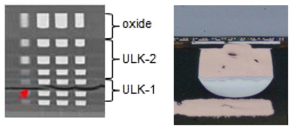
- Low-k materials are mechanically weak & porous but are essential to reduce RC delay and cross talk in BEOL layers.
- Thermo-mechanical stress can can induce “white bump” failure (low-k dielectric damage), dielectric layer delamination and thus bump crack and UBM peeling.
- Moisture absorption/diffusion into the low-k dielectric layer also impacts the CPI performance.
- BEOL film layers adhesion strength is very critical for package reliability.
- Bump structure integrity (observed by cross section imaging) & BEOL film structures integrity are measured using thermo-mechanical and environmental stress test conditions.
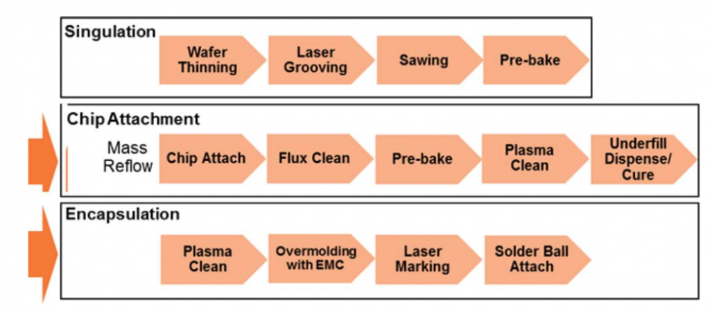
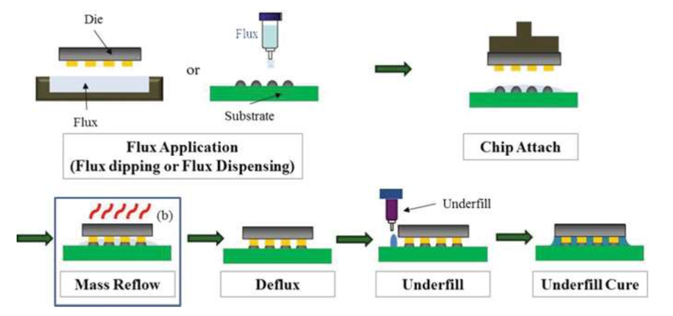
- Mass reflow chip attach process is cost effective solution for packaging but has higher risk of bump to trace shorts & solder bridging especially for finer bump pitch (<60um) & finer LW/LS with the escaped traces. It also induces higher thermal stress on whole package.
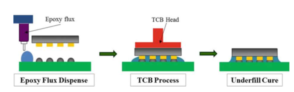
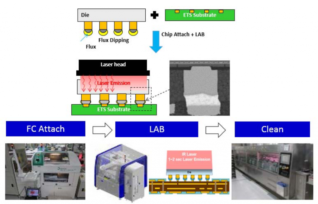
- Thermo Compression Bonding (TCB), Laser Assisted Bonding (LAB) are other alternatives to mass reflow bonding process but cost and throughput will be impacted.
- LAB can increase throughput UPH (unit per hour) by more than 2 times than TCB technology.
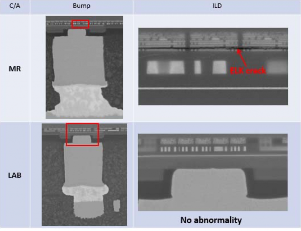
- LAB chip attach technology helps better to reduce the risk of low-k dielectrics delamination compared to TCB and MR process as laser can be targeted only in the region of interest.
- Increased die sizes, finer interconnect pitches, higher I/O counts along with the ultra & extreme low-k materials poses greater risk for the CPI reliability.
- Better package design, proper material selection and optimized assembly processes will be required to minimize the CPI risk.
- Typically, CPI reliability assessments are performed with the below test conditions to check the strengths of the structures.
| Test Method | Test Condition | Cycle/hour |
| Precon | 30ºC/60% RH/RT~ 260ºC | 96 Hrs/3 cycles |
| uHAST | 130ºC, 85%RH, 2.3atm | 100 hrs |
| TCT | -55ºC ~ 125ºC | 1000 cycles |
| TST | -55ºC ~ 125ºC | 500 cycles |
| HTST | 150ºC | 1000 hours |
References:
- Hsu, C. Chen, S. Lin, T. Yu, N. Cho and M. Hsieh, “7nm Chip-Package Interaction Study on a Fine Pitch Flip Chip Package with Laser Assisted Bonding and Mass Reflow Technology,” 2019 IEEE 69th Electronic Components and Technology Conference (ECTC), Las Vegas, NV, USA, 2019, pp. 289-293, doi: 10.1109/ECTC.2019.00050.
- Shan Gao et al 2015 ECS J. Solid State Sci. Technol. 4 N3134.
- P. C. Kuo, C. H. Wang, K. K. Ho, K. M. Chen, C. Y. Wu and C. L. Yang, “14 nm chip package interaction development with Cu pillar bump flip chip package,” 2015 IEEE 65th Electronic Components and Technology Conference (ECTC), San Diego, CA, 2015, pp. 30-34, doi: 10.1109/ECTC.2015.7159567.
- Lee S. (2017) Fundamentals of Thermal Compression Bonding Technology and Process Materials for 2.5/3D Packages. In: Li Y., Goyal D. (eds) 3D Microelectronic Packaging. Springer Series in Advanced Microelectronics, vol 57. Springer, Cham. https://doi.org/10.1007/978-3-319-44586-1_7.
Leave a Reply