
Electromigration is a mass transport process due to momentum exchange between the mobile valence electrons and atoms (ions). During the current flow in the conductor, valence electrons bumps into the atoms (ions) and moves the atoms (ions) in the direction of the electron movement constituting an electromigration.
- The effect is more pronounced due to higher current density in shrinking IC feature size.
- The momentum transfer between the valence electrons and metal ions occurs due to the imperfection of the crystal structure in the metals such as lattice vacancy and other defects, lack of symmetry in grain boundaries & material interfaces, higher thermal vibration etc.
- Due to the imperfection and lack of symmetry in the irregular crystal lattice, the metal ions are bonded weakly, and the momentum transfer is more vigorous.
- Uniform lattice structure of metal ions in homogeneous crystalline structure, there is hardly any momentum transfer from valence electrons and metal ions.
- In ideal conductor, atoms are arranged in perfect crystalline structure with no grain boundaries & no lattice vacancy, there is no collision of electrons with atoms and there will be no electromigration.
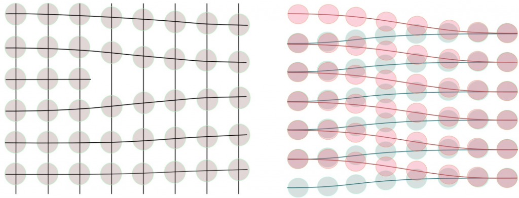
- When the electron wind strength passes certain threshold, the ions gets separated from the grain boundaries and transported in the direction of the current.
- The dislodged ions tend to move along the grain boundaries.
- Normally, in the case of low current density; there will not be enough electron strength to bombard the ions to dislodge them permanently. However, if many electrons impart significant force in the imperfect lattice sites in the crystal, the ions can be knocked out from its position and this constitutes the electromigration.
- Joule heating due to higher electrical resistance and higher current density also contributes to the electromigration.
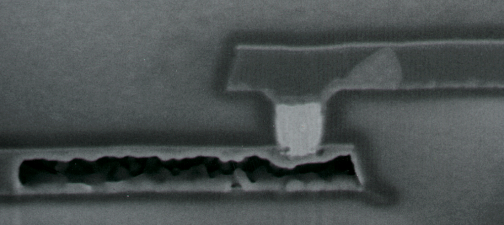
- The knocked-out ions from its original position in the conductor eventually creates two fail modes in the electronic system – open circuit failure and short circuit failure.
- Even before open circuit failure, the voids also impacts mechanical and structural integrity of the device or package.
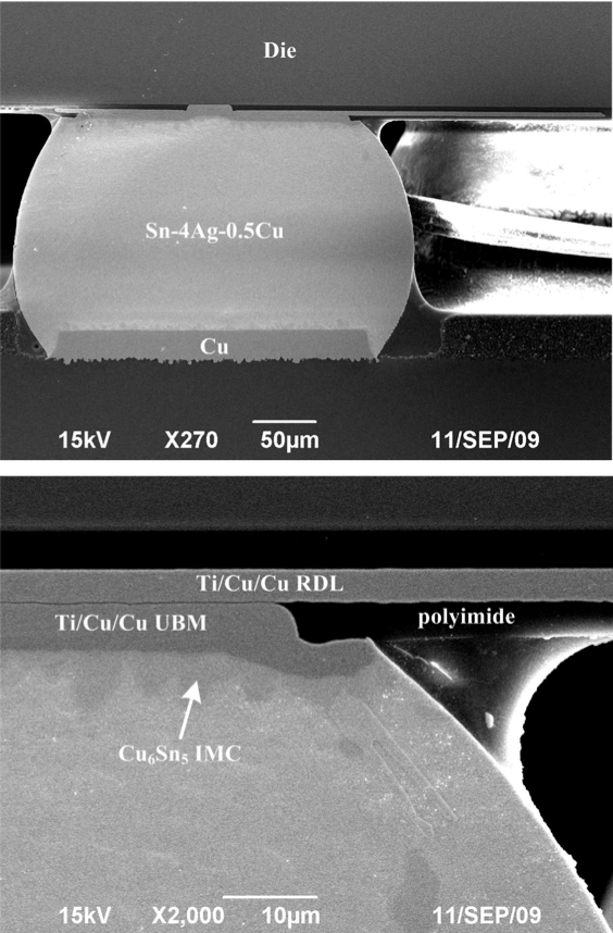
- In WLCSP package, dies are directly mounted to the PCB thus providing better electrical and thermal performance due to shorter interconnection lines.
- 3 approaches for the WLCSP bumping – Direct connection of bumps to the underlying die pads without repassivation, Bump on pad (BOP) with repassivation & Bump on redistributed line pad.
- RDL lines serves as electrical and thermal path.
- Decrease in the bump pitch and increase in the I/O count leads to increase in the current density. Higher current density in turn leads to current crowing and Joule heating in the vicinity of the solder joint and UBM structure leading to the increase in resistance.
- The increased resistance is due to the structural damage of the RDL lines, UBM or UBM/Solder joints due to electromigration.
- UBM/Bump metallurgy can be modified to incorporate barrier layer such as NiAu to retard the intermetallic compound (IMC) growth which eventually reduces the electromigration.
- IMC will be formed on both chip and board sides of the device after reflow.
- Higher temperature will have a higher impact than current density on electromigration lifetime as higher operating temperature leads to fast ionic diffusion.
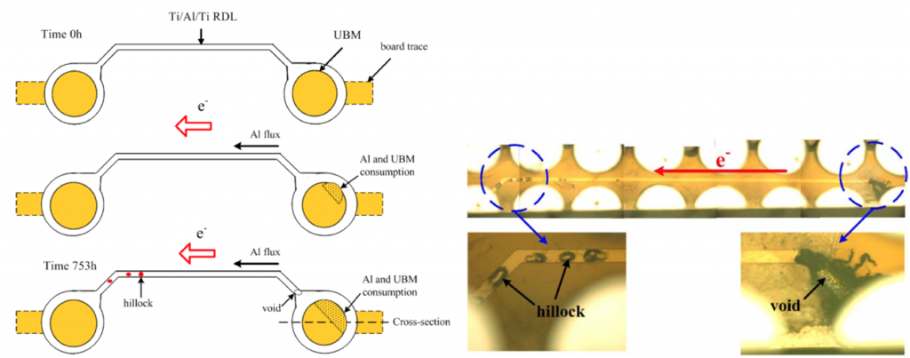
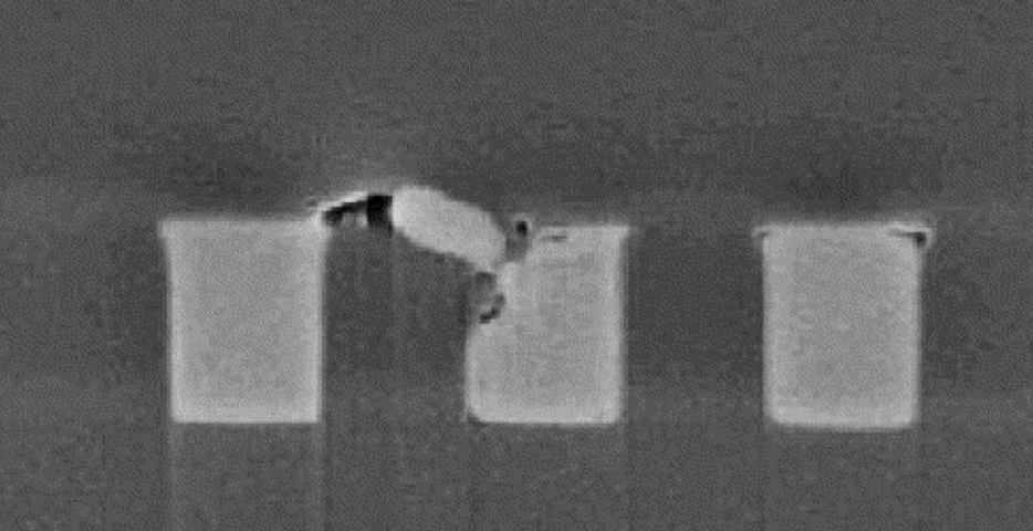
- Current stressing causes voids to nucleate around cathode area of RDL/UBM and hillocks around anode area due to mass transport. Thus the RDL, UBM layers gets consumed due to stressful operating conditions and leads to voids and hillocks.
- Voids leads to decrease in the cross-sectional area of the RDL/UBM and leads to temperature increase due to Joule heating.
- Polyimide around the voids also experiences degradation due to localized increase in temperature.
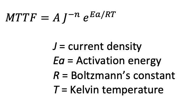
- Electromigration is the major interconnect reliability issue. The failure lifetime of a metallic conductor can be modelled by Black’s equation under current stressing condition.
- Black’s equation provides the simplest way to measure the mean time to failure (MTTF) due to electromigration.
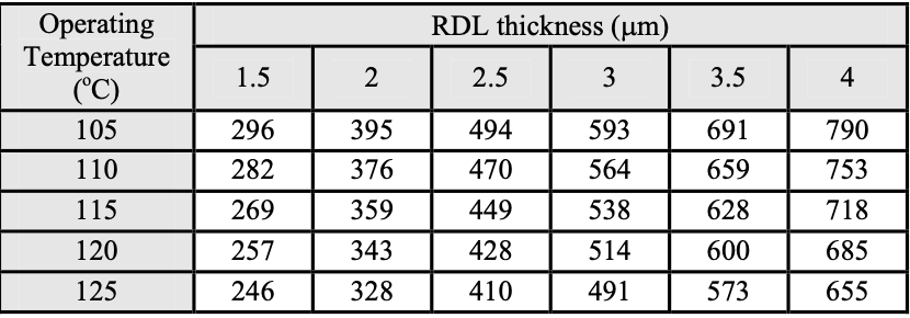
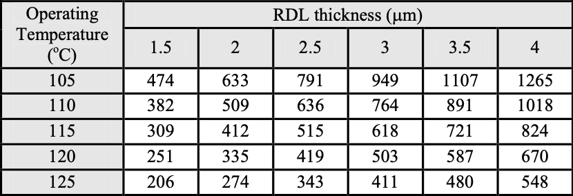
- Example – with Weibull characteristics lifetime, max allowed current (mA) for the sputtered Ti/Al/Ti ( 0.2um/1.5um/0.2um) and sputtered & electroplated Ti/Cu/Cu (0.1um/0.2um/5um) RDL for 100k hours continuous operation without electromigration:
References:
- Zhao, H. (2018). FEM Based Multiphysics Analysis of Electromigration Voiding Process in Nanometer Integrated Circuits. UC Riverside. ProQuest ID: Zhao_ucr_0032D_13581. Merritt ID: ark:/13030/m5c29txx. Retrieved from https://escholarship.org/uc/item/41f4p23x.
- Kao, Chin Li ; Chen, Tei-Chen ; Lai, Yi Shao ; Chiu, Ying Ta. / Investigation of electromigration reliability of redistribution lines in wafer-level chip-scale packages. In: Microelectronics Reliability. 2014 ; Vol. 54, No. 11. pp. 2471-2478.
- Scotti, Gianmario. (2008). Electromigration in Solder Interconnects.
- R. Plieninger, M. Dittes, K. Pressel, “Modern IC packaging trends and their reliability implications, Microelectronics Reliability”. https://doi.org/10.1016/j.microrel.2006.08.008
- JR Lloyd. Electromigration in integrated circuit conductors.Journal of Physics D:Applied Physics, 32(17):R109, 1999.
- Christine S Hau-Riege. An introduction to cu electromigration.Microelectronics Reli-ability, 44(2):195–205, 2004.
- Y. Lai, C. Kao, Y. Chiu and B. K. Appelt, “Electromigration reliability of redistribution lines in wafer-level chip-scale packages,” 2011 IEEE 61st Electronic Components and Technology Conference (ECTC), Lake Buena Vista, FL, 2011, pp. 326-331, doi: 10.1109/ECTC.2011.5898533.
Leave a Reply