
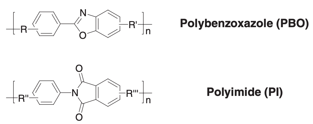
Polyimide (PI) and Polybenzoxazole (PBO) products are typically used as a stress relief and protective insulating layer before packaging or redistribution layer (RDL).
PI and PBO plays a critical role in advanced microelectronic packaging as an insulating material and can be processed as a standard photolithography process. Conventionally, photoresist was used on top of the PI/PBO polymer to develop the etching pattern, but to simplify the manufacturing process & cost, photosensitive PI/PBO polymer were developed later on. These polymers possess several outstanding features such as high thermal stability, chemical resistance, low flammability & low dielectric constant for the use in advanced packaging technology. Relatively, PBO’s has lower dielectric constant and lower moisture absorption due to the absence of carbonyl group in their polymer backbone.
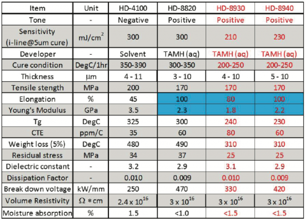
PI/PBO polymers can be developed into both positive and negative tone. Typically, PI polymers are negative acting and solvent developable during the exposure of i-line or broadband UV spectrum. In the negative tone, the exposed area becomes insoluble to the developer solution and only unexposed area becomes soluble. The pattern or remaining polymer layer is thermally cured to produce the PI film pattern. On the other hand, PBO’s generally are positive- acting and aqueous developable materials which are soluble in alkaline developers such as 2.38% tetramethylammonium hydroxide (TMAH). Diazonaphthoquinone (DNQ) photoacid generators are used for pattering which provides better contrast during exposure and development. The DNQ undergoes Wolff rearrangement during exposure of UV light energy and changes to indene carboxylic acid (ICA). This change helps to improve both the dissolution rate and contrast during development. The unexposed pattern is then thermally cured to obtain the robust PBO film.
There are no significant performance differences between both PI and PBO polymers and their choice depends on the specific need of the end product requirements such as via diameter, Cu trace thickness etc. In general, positive acting system provides better resolution of via or line/space whereas negative active system is more well suited for the thicker film thickness requirements. DNQ photoacid generator in positive acting system has very high UV wavelength absorption (higher optical density ~ 4) and thus light is absorbed deeper into the film providing better resolution compared to the negative acting system (lower optical density ~ 0.5).
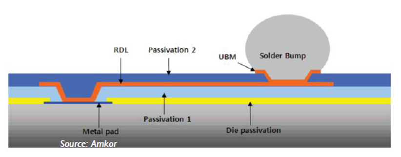
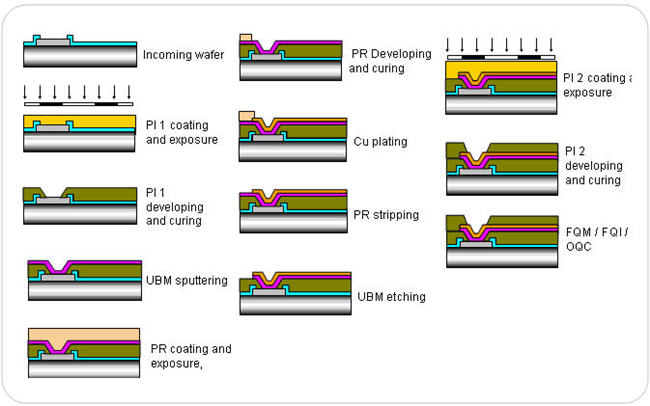
PI/PBO polymers are extensively used as a dielectrics and passivation layers in different bumping and redistribution layer (RDL) technology in wafer level packaging & flip chip chip scale pakage (FCCSP) products where high I/O density is paramount. There can be multi-layers of these polymers in varying thickness in the wafer bumping process with or without RDL structure. The process temperature regime to cure these polymers during these fan- in wafer level packaging (WLP) processes are more forgivable and can go beyond 300°C without much negative consequences in devices since full package structures are not completed yet. However, in advanced Fan-Out Wafer Level Packaging (FO-WLP) technology, the redistribution layers are fabricated on the mold compound reconstituted wafer, the PI/PBO polymer cure temperature needs to be less than the glass transition temperature (Tg) of the mold compound which is in the range of 150°C –175°C. Due to this lower process temperature requirement for RDL structure in advanced Fan-Out packaging, the PI/PBO polymers needs to be cured below Tg of mold compound without impacting the reliability of the packages. This low curing temperature requirement presents significant challenges in advanced Fan-Out packaging technology and key requirement & challenges in PI/PBO polymer technologies are listed below.
- PI/PBO polymer redesign for low curing temperature – Lower processing temperature ensures no impact on mold compound and die & is always desired to reduce the package warpage induced failures. Moreover, the post application curing temperature needs to be lower than lowest Tg of the package materials, usually the organic mold compound (<200°C) with robust thermal, chemical and electrical performance required in FO-WLP.
- Polymer thickness after cure – Depending on the end applications, Cu RDL can be of varying thickness and PI/PBO polymer thickness needs to properly insulate the Cu RDL thickness (~ 3 – 30um).
- Finer resolution – With the increasing I/O density and finer pitch in advanced microelectronic devices as well as increasing use of Fan-Out technology not only in discrete components but in application processors, PI/PBO polymer technology needs be developed with lithography resolution <5um of via openings to meet the challenge.
- Sidewall slope shape – Steep slope imparts higher stress on the top corner edge of the solder bump and should be avoided. In this regards, cured PI/PBO having a smooth profile with no crowning at the top edge of the sidewall and the sidewall angle of 70-75° acute angle to the substrate is preferable.
- Elongation (high-stretch, low-stress polymer) – A higher elongation % material property of PI/PBO provides more cushion and less stress on the material during extreme operating conditions such as temperature cycling test and prevents cracks within the dielectric and metal dielectric interface.
- Chemical resistance – The bumping, RDL and overall fabrication processes involves many intensive chemical process steps such as photo resist stripping, plating, etching and use of acidic fluxes. The PI/PBO polymers needs to chemically stable and withstand those diverse chemical processes.
- Good adhesion to metal surfaces – Delamination of the inter-layer dielectrics and metal-dielectric interface is one of the common and most challenging reliability issue. The PI/PBO polymers after low temperature cure needs to have good adhesive strength for the reliable performance of the package.
- Good insulation with low dielectric constant/dielectric loss – The main function of PI/PBO polymers is to insulate the multiple fine line & space (L/S) Cu trace layers. The polymer needs good insulating property along with low dielectric constant (k) not to degrade the electrical performance of the package.
References
- Fukukawa, K., Ueda, M. Recent Development of Photosensitive Polybenzoxazoles. Polym J 38, 405–418 (2006). https://doi.org/10.1295/polymj.38.405
- http://www.chipbond.com.tw/eng_service_03_02.aspx
- Polyimide and polybenzoxazole technology for wafer-level packaging, Chad Roberts, HD Microsystems, Chip Scale Review, July-August, 2015 p. 26-31.
- Enomoto, T., Matthews, J. and Motobe, T. (2020). Advanced Dielectric Materials (Polyimides and Polybenzoxazoles) for Fan‐Out Wafer‐Level Packaging (FO‐WLP). In Advances in Embedded and Fan‐Out Wafer‐Level Packaging Technologies (eds B. Keser and S. Kroehnert). doi:10.1002/9781119313991.ch14
Leave a Reply