Wafer Dies: Microelectronic Device Fabrication & Packaging

Semiconductor Device Fabrication, Assembly & Packaging Notes

  • Home
  • IC Packaging Reliability
  • Semiconductor Assembly & Packaging
  • Fabrication & Packaging Materials
  • Semiconductor Process Technology
  • About Us
  • Privacy Policy

Wafer Singulation

Die Prep Process Overview

August 30, 2020 Resham Thapa 1

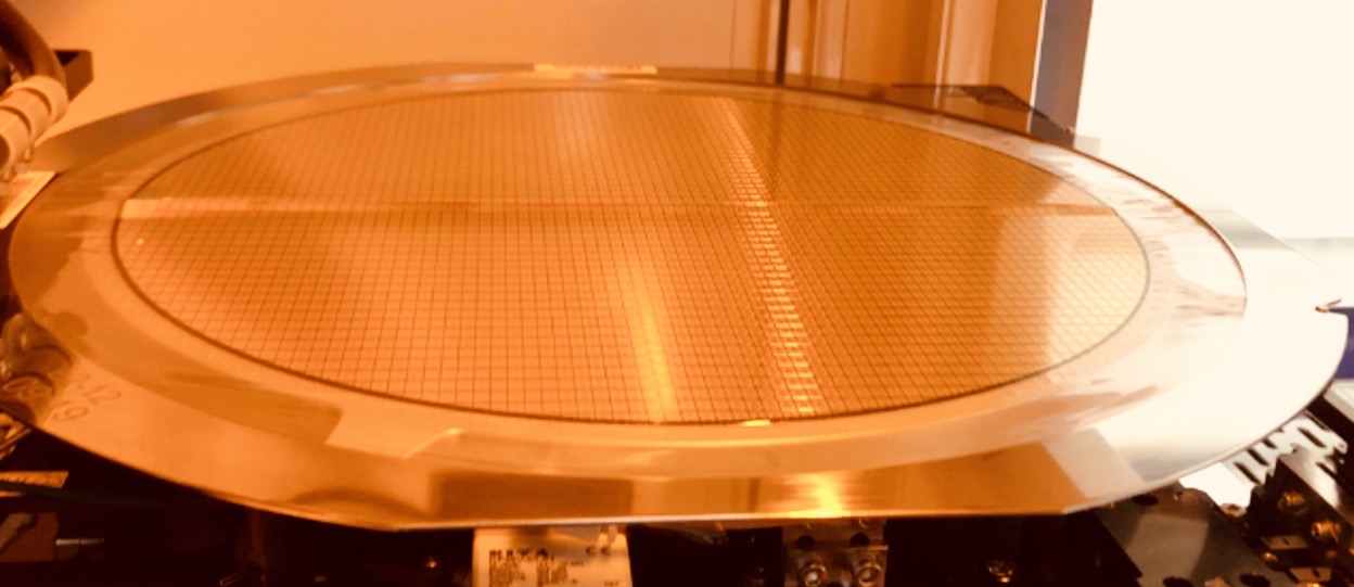
The journey of a semiconductor integrated chip (IC) begins with the design of the IC, manufacturing of the wafer by imprinting the circuits and devices […]

Recent Posts

  • Polyimides (PI) & Polybenzoxazoles (PBO): Advanced Dielectric Polymers for Wafer Bumping & Wafer Level Packaging
  • Solder Joint Fundamentals in Wafer Bumping & Packaging
  • Electromigration in WLCSP Packaging
  • Chip Package Interaction (CPI) in Flip Chip Package
  • Die Prep Process Overview

Categories

  • Fabrication & Packaging Materials
  • IC Packaging Reliability
  • Semiconductor Assembly & Packaging
  • Semiconductor Process Technology

Copyright © 2025 | WordPress Theme by MH Themes